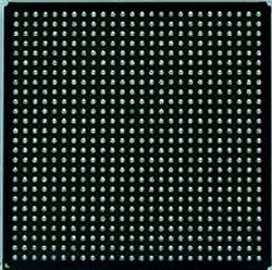
PROVIDING TOP-NOTCH IC DESIGN AND MANUFACTURING
Silicon Artist™ designs custom chips for the world’s leading electronics companies. Offering the industry’s most flexible engagement model, our experienced design teams provide expertise at each step from specification through delivery of qualified, packaged, tested, custom chips. Silicon Artist™ offers value added design expertise, with an infrastructure that provides significant predictability and time-to-market advantages. We ensure a high quality, full-support customer experience that results in the fastest and most cost effective path to silicon for companies of all sizes. Silicon Artist™ leverages it’s tier one supply chain partners to deliver technology and pricing advantages and improved product visibility.
IC Design & Manufacturing Silicon Art assists leading and emerging semiconductor companies improve their design, manufacturing strategies, and methodologies with proven results in IC Design & Manufacturing. We’ll manage the logistics from any IP provider with customized IC manufacturing supply chains.
Digital Design and Physical Implementation
Clients that hand-off an implemented design in GDS format having passed DRC and LVS physical verification checks utilize Silicon Artist‘s COTxPress™ program.
Silicon Artist Program Managers, Engineers and Partners remove the complexity and internal resource challenges of the flexible and profitable Customer Owned Tooling (COT) path by providing world class operations consultation in concert with best in class supply partners to oversee the delivery of prototype and volume packaged, tested & characterized ICs.
In this partnership model, Silicon Artist provides consultation on wafer fabrication, assembly, test, qualification, characterization, and volume parts shipment. COTxPress™ includes consultation on prototype delivery through production volume, utilizing the process technology, which best fits, your design. All test program development is also included in this model. Let our experienced Team manage the process for you.
Standard Silicon Artist Services included with a COTxPress™ engagement include:
-
- Mask Set Generation
- Wafer Sort, Characterization, Final Test, and QA Test Program Development
- ATE and Bench Test Load Boards, Probe Cards, Socket and Package Custom Tooling
- Design of Burn in Board (s)
- Product process and package qualification and summary report to include data for the following battery of tests:
- HAST
- HTOL
- 85/85
- Thermal Shock
- Temperature Cycling
- HTS
- ESD
- Latch up
- Product Characterization to Include
- Corner Lot Manufacturing
- Characterization Plan Generation
- Summary Report
- Manufacturing Consulting
- Assembly
- Final Test
- Shipment of Prototypes
- Production Shipment Logistics
-
In the ASICxPress™ engagement model, Silicon Artist provides both IC design & supply chain consulting services to our customers. Customers perform the logic design and then provide Silicon Artist with a netlist and timing requirements. We will manage the entire process, from netlist handoff to setting up a supply chain for delivery of packaged, tested parts.
Silicon Artist‘s experienced design team takes responsibility for the physical implementation, and our seasoned supply chain operations consultants will oversee fabrication, assembly, test, and product engineering through prototype delivery, product qualification and production shipments.
Standard Silicon Artist Services included with an ASICxPress™ Netlist Handoff engagement
-
- Design for Test and Scan Chain Optimization Consultation
- Physical Implementation (Floor Planning, P&R) & ECO
- Parasitic Extraction, Post-Layout Timing Verification
- Pre and Post-Layout Formal Verification
- Design and Signal Integrity Analysis (Crosstalk, IR Drop and Electro-migration)
- Pin-out and Power/Ground Distribution Analysis
- Simultaneous Switching Output Analysis
- Substrate Noise Analysis
- GDS-II Generation, Layout Verification & Design Rule Checking
Plus all the services we provide to our COTxPress™ customers, including:
-
- Mask Set Design
- Test Program Generation
- Wafer Sort, Final Test, Characterization, and QA Test Program Development
- Prototype Test, Product Characterization, and Reliability Test Development
- Load Board, Probe Card, Socket and Package Custom Tooling Design
- Burn-In Board & Socket Design
- Tester Access for Test Development
- Consulting on Manufacture, Test and Shipment of Prototypes Consulting
-
Silicon Artist‘s PROTOxPress™ service helps reduce project risk by allowing you to validate your design in silicon before paying for a full mask set. By using multi-project wafer technology from industry leading suppliers, Silicon Artist can quickly produce your IC prototypes. Customers may purchase up to 2,000 of these prototype parts, in the package of their choice, for a fraction of the cost of a full-mask-set prototype wafer run. Silicon Artist also offers a full range of custom prototyping services through the PROTOxPress™ program.
As market pressures, mask costs and cycle times for advanced IC technologies continue to increase, the financial and time-to-market imperative of “right the first time” becomes a matter of survival. In many cases, a low cost, fast turnaround path to prototype units may be the only way to guarantee successful production.
Silicon Artist™ addresses this need with its PROTOxPress™ service. PROTOxPress™ allows you to provide engineering samples to your customers (and your engineering team) at the earliest possible time. You no longer need to deal with the performance uncertainties of an FPGA-based prototype. Before placing a volume order, you get your design, in your package, validated in your system.
You also reduce the risk associated with re-spins due to design and/or IP integration issues. At 28nm, those risks can be substantial; the cost of PROTOxPress™ validation before release to production can be half of the cost of a full production re-spin. PROTOxPress™ allows you to “silicon verify” all of your IP before production begins.
Features & Benefits
* PROTOxPress™ is designed to minimize the time, effort and manpower required for prototypes
* Using multi-project wafer technology, Silicon Artist drives down the cost of your prototype units
* We also can provide a comprehensive range of engineering services that reduces your team’s time and effort required to migrate approved prototypes to full production manufacturingThe steps that occur in every PROTOxPress™ engagement include:
* Validation of the design’s manufacturability
* Enhancement/remediation of design manufacturabilityIn short, Silicon Artist provides everything you need for a fast and reliable rapid prototyping engagement using the most advanced multi-project wafer technology.
Availability
Silicon Artist is currently accepting PROTOxPress™ engagements.Silicon Artist supports a wide variety of package vendors and package types for PROTOxPress™ devices as well as bare die and back lapped die for customer assembly. Individual orders of between 40 and 2000 prototypes are welcomed.
Silicon Artist is RF capabilities: our designers bring 4 critical areas of expertise to RF analog design
1) High Levels of Integration
-
- RF sections in CMOS
- Minimizing IC interconnects with entire SoC
2) Low Power
-
- IC Architecture
- Minimize Down Conversion Stages
- Eliminate Chip Interconnects
- Block/Module design expertise
- LNA
- PA
- Mixers
- Freq Dividers
- PLL
- IC Architecture
3) Cost Effective Design Techniques
-
- Innovative Circuit Designers
- Experienced Layout Team
4) Complete Turnkey RF/SoC IC design understanding and execution
-
- Specification Development or Review
- Transistor Level Design
- Detailed Layout for manufacturing
- Test Architecture and program development
Additional evidence: ICs completed by Silicon Artist team members include:
Lowest Power GPS IC: Valence VS7001
2 different published papers authors are Silicon Artist engineers
High Frequency (6GHz) WIFI IC – 802.11a/b/g
1st GSM (TDMA) IC in early 90s – Phillips SA1638
Additional Phillips ICs – NE605, NE607, NE608, NE62
-
Silicon Artist performs CAD services for clients including: Process Design Kit (DRC, Extraction, Antenna, Simulation Models, extraction, cell parameterization) development/enhancement, script development, tool selection/integration, library development/maintenance/migration and reference EDA flow validation.
Analog & RF IP design, retargeting existing IP, IP contract negotiations and hardening of RTL IP for new processes and foundries.
Custom Outsource activities tailored to our clients needs in the areas of analog, digital & mixed signal design implementation, layout, and physical verification. Onsite and Off-site IC Design and Layout engineers, tools and analog and RF block integration.
Analog Block Design and Layout
IC Production Consulting
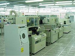
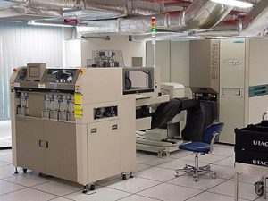
Silicon Artist IC Production Consulting services includes post production capabilities including: testing, analysis, and reliability qualification services. We are capable of providing turn-key FA analysis, testing and qualifications for large projects or accomplishing single event analysis services. IC Manufacturing outsourcing is the solution for fabless and IDM semiconductor companies looking to reduce cost, time, and overhead.
Silicon Artist is pleased to provide the following post production services:
Reliability Qualification Testing
The purpose of reliability testing is to ensure that products are properly designed and assembled by subjecting them to stress conditions that accelerate potential failure mechanisms. Reliability test methods are defined in many industrial standards, such as MIL-STD-883 and JEDEC STD-22.
Silicon Artist provides for the following reliability qualification test services:
* HAST (Highly Accelerated Temperature and Humidity Stress Test)
* Thermal Shock (Liquid to Liquid)
* Autoclave or Pressure Cooker Test
* Temperature Cycling (TC) Air to Air
* Temperature Humidity Bias Lifetest 85C/85%
* Humidity-Bias Test (THB)
* HTOL (High Temperature Operating Lifetest) / Burn-in
* High-Temperature Storage Life Test (HTSL)
* Bias Life Test (BLT)
* Preconditioning
* Real Time Thermal Profiling
* Solderability
* Fine and Gross Leak Testing (Seal)
ESD and Latch-up Testing
Silicon Artist can support any post manufacturing ESD and Latch-up testing requirements. In addition to reliability testing, we can provide ESD and Latch-up failure analysis to identify events and point of entry using the latest in fault isolation techniques, including:
* Human Body Model (HBM) testing
* Machine Model (MM) testing
* Charged Device Model (CDM) testing
* Latch-up testing
FIB Circuit Modifications
Silicon Artist is with you throughout your IC project. Even if ever the unthinkable interferes with you project schedule. The FIB systems we work diligently to never have to use provide for platinum metal deposition, dielectric insulator deposition, and enhanced etch chemistries. If needed we can provide for:
Circuit Modifications – Copper and latest geometry technology modifications. Cut and jump IC modification is a cost efficient method to debug and make design changes prior to re-masking.
Probe Pads – Deposit probe points for electrical characterization that are not accessible via conventional probing techniques.
Wire Bond Pads – Deposit wire bonding pads for high current modifications.
Precision Cross Sections – Perform precision cross sections with sub micron accuracy. Cross section photo resist, MEMS, and biological structures that do not lend themselves to conventional mechanical cross section techniques.
TEM sample preparation – Thin cross section samples for subsequent TEM imaging.
Failure Analysis
* Device Level FA
* System Level FA
* Light Emission Microscopy (LEM)
* Thermal Infrared Imaging
* Externally Induced Voltage Alterations (XIVA)
* Transmission Line Pulse Testing (TLP)
* DC Characterization
* Mechanical Microprobe
* Scanning Electron Microscopy (SEM)
* Energy Depressive Spectroscopy (EDS)
* High Resolution Real Time X-ray Imaging
* High Resolution Scanning Acoustic Microscopy (SAM)
* Wire Bond and Solder Ball Bond Strength Testing
* Device Construction Analysis
* Sample Preparation Services
- Backside Sample Milling
- Parallel Lapping
- Cross-section
- Device Decapsulation
- Plasma Etching
- Laser Cutting
Stacked Die
Die Bumping
MCM
Pin Grid Array
BGA HS 35×35
Assembly
Coming Soon